English
  日本語
日本語  한국어
한국어  français
  Deutsch
  Español
  italiano
  русский
  português
  العربية
  ไทย
ไทย 
In the intricate realm of semiconductor manufacturing, precision and accuracy are not just desirable – they are paramount. As technology advances and semiconductor components become increasingly sophisticated, the need for advanced metrology tools is more critical than ever. Telecentric zoom lenses, often unsung heroes in this field, play a pivotal role in ensuring that semiconductor manufacturing reaches new heights of precision. In this blog post, we unravel the significance of telecentric zoom lenses in semiconductor metrology and how they go beyond clarity in shaping the future of microelectronics.
Semiconductor components are characterized by minuscule dimensions and intricate structures. Telecentric zoom lenses, with their ability to provide distortion-free and uniform magnification, redefine the standards for dimensional measurement. In semiconductor metrology, where every nanometer counts, these lenses contribute to ensuring that each component meets exacting specifications, paving the way for the next generation of microelectronics.
The semiconductor industry operates on razor-thin margins, and any defects in the manufacturing process can have profound consequences. Telecentric zoom lenses, with their advanced imaging capabilities, contribute to defect detection with unrivaled accuracy. Whether it's identifying microscopic anomalies or ensuring the uniformity of patterns, these lenses play a crucial role in enhancing semiconductor yield and reducing production costs.
Inspecting the surfaces of semiconductor wafers demands a level of precision that conventional lenses may struggle to achieve. Telecentric zoom lenses, by providing a clearer and distortion-free view, illuminate critical inspection points on wafer surfaces. This heightened visibility is instrumental in identifying imperfections, contaminants, or irregularities that could compromise the functionality of the final semiconductor product.
From the designer's perspective, telecentric zoom lenses offer a unique advantage in the visualization of microelectronic components. Designers can work with greater confidence, knowing that the intricate details of their designs will be accurately replicated during the manufacturing process. This alignment between design intent and manufacturing output is crucial in creating cutting-edge microelectronics.
In conclusion, telecentric zoom lenses are catalysts for progress in semiconductor metrology. Beyond providing clarity, these lenses redefine the parameters of precision, defect detection, and microelectronic design. As the semiconductor industry continues to evolve, the role of telecentric zoom lenses will undoubtedly become even more pronounced, setting new benchmarks for the future of microelectronics.
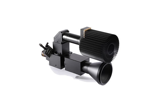
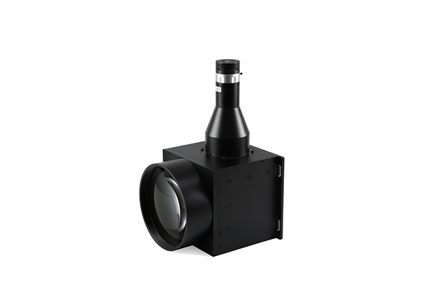
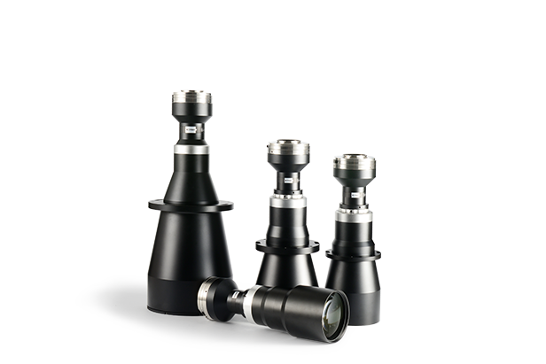
Related Machine Vision Telecentric Lens Products