English
  日本語
日本語  한국어
한국어  français
  Deutsch
  Español
  italiano
  русский
  português
  العربية
  ไทย
ไทย 
In the world of digital technology, semiconductors play a crucial role in powering our devices. From smartphones to laptops, semiconductors are the building blocks that enable the functionality we have become dependent on. However, the production and quality control process for semiconductors is an intricate one, demanding high precision and accuracy. This is where telecentric imaging systems come into play, revolutionizing the way semiconductor inspections are conducted.
A telecentric imaging system is an advanced optical setup that ensures accurate and reliable measurements. Unlike traditional imaging systems, where objects closer to the lens appear larger, telecentricity maintains consistent magnification irrespective of an object's distance from the lens. This unique characteristic of telecentric lenses eliminates any distortions caused by the variations in object distance, allowing for precise measurement and inspection.
One of the primary applications of telecentric imaging systems in the semiconductor industry is in wafer inspection. Before semiconductors are sliced into individual chips, they are first produced on a silicon wafer. It is vital to inspect these wafers thoroughly to ensure the absence of any defects that could impact the functionality and reliability of the final chips. Telecentric lenses provide accurate and distortion-free image viewing, making it easier for inspectors to identify even the tiniest anomalies on the wafer surface.
Another area where telecentric imaging systems are widely utilized is in the measurement of microscopic structures on semiconductor chips. One of the critical measurements in semiconductor manufacturing is the width of features on the chip, such as circuit lines. These measurements need to be extremely precise, as even the slightest variation can affect the chip's performance. Telecentric lenses enable accurate measurement by maintaining a constant magnification, irrespective of the position of the features on the chip. This ensures that the measurements obtained are reliable and consistent.
Furthermore, telecentric imaging systems are also vital in detecting defects in semiconductor chips. Defects can arise during the manufacturing process, which, if not identified, can result in faulty chips. With the help of telecentric lenses, defects such as scratches, cracks, or debris can be easily detected and analyzed. The distortion-free images provided by telecentric imaging systems assist in accurate defect identification, leading to improved quality control in semiconductor production.
The benefits of telecentric imaging systems in semiconductor inspection are evident. The accuracy and precision provided by these systems contribute to enhanced quality control, reduced production wastage, and improved overall productivity. Furthermore, the distortion-free images obtained through telecentric lenses enable inspectors to make reliable decisions based on accurate measurements and defect identification.
In conclusion, telecentric imaging systems have unleashed a new era in semiconductor inspection. The ability to maintain consistent magnification, regardless of object distance, has revolutionized the way semiconductors are inspected and measured. From wafer inspection to defect detection, these advanced optical systems offer unparalleled precision and accuracy. As the semiconductor industry continues to evolve, telecentric imaging systems will undoubtedly play a pivotal role in ensuring the production of reliable and high-quality semiconductor chips.
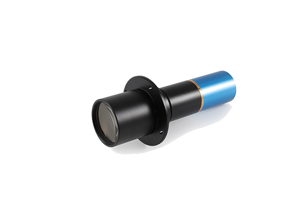
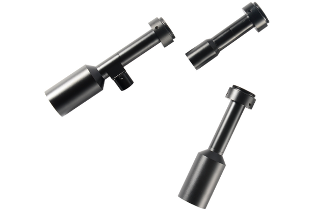
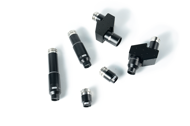
Related Machine Vision Telecentric Lens Products